Page 2 - A Closer Look

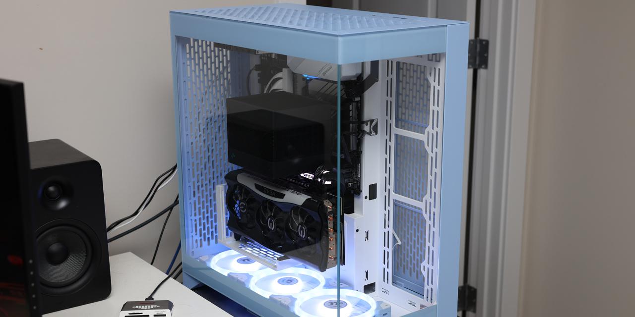
Wow, the Asus EAX1950PRO is huge. The length of the PCB as obtained from our measurement is approximately 23.5cm; roughly the length of a 8800GTS. One of the most prominent problems we've seen in this regard is the placement of PCIe power connector located at the end of the card -- users with smaller cases might have to remove the hard drive cage in order to plug in the power connector, or may interfere with motherboard IDE connectors. However, I had no problems with my Thermaltake Aguila in terms of installation and usage, and the Asus EAX1950PRO did not block out anything on our Asus P5W64-WS Professional.
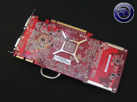
The back of Asus X1950 Pro's PCB. The large heatsink is held down by four screws and the bracket; which can easily be removed without any hassles -- as long as you have a properly sized and compatible screwdriver. Yes, I wrote compatible.

Removing the heatsink reveals the core, as well as a total of eight memory chips. The heatsink cools down all memory chips with a thermal pad acting as a contact medium. Thermal paste is applied to the X1950 Pro GPU core.
The Asus heatsink features a single heatpipe. The heatpipe transfers heat to the end of the heatsink located between the fins for the fan to push the warm air out.

A closer look at the shiny X1950 Pro chip. The GPU is a RV570 (215PADAKA12FG); meaning it has a 80nm die size. Further specifications include:
GPU: RADEON X1950 PRO (RV570)
Interface: PCI-Express x16
GPU clock rate: 581MHz
Memory clock rate: 700MHz DDR (1.4GHz effective)
Memory bus: 256-bit
Vertex shader processors: 8
Pixel shader processors: 36
Texture processors: 12
ROPs: 12
PCB color: Red
Outputs: 2 x DVI (Dual-Link), TV Out
TV-out: Yes
Multi-GPU operation: CrossFire (integrated into GPU)

A shot at 2 of 8 Samsung K4J55323QG memory chips aboard Asus' X1950 Pro. Each chip is 32MB of GDDR3 RAM; with further information obtained from Samsung's site:
FOR 2M x 32Bit x 4 Bank GDDR3 SDRAM
The K4J55323QG is 268,435,456 bits of hyper synchronous data rate Dynamic RAM organized as 4 x 2,097,152 words by 32 bits, fabricated with SAMSUNG's high performance CMOS technology.
Synchronous features with Data Strobe allow extremely high performance up to 6.4GB/s/chip.
I/O transactions are possible on both edges of the clock cycle.
Range of operating frequencies, and programmable latencies allow the device to be useful for a variety of high performance memory system applications.
Features
1.8V± 0.1V power supply for device operation
1.8V± 0.1V power supply for I/O interface
On-Die Termination (ODT)
Output Driver Strength adjustment by EMRS
Calibrated output drive
1.8V Pseudo Open drain compatible inputs/outputs
4 internal banks for concurrent operation
Differential clock inputs (CK and /CK)
Commands entered on each positive CK edge
CAS latency : 4, 5, 6, 7, 8, 9, 10, 11 (clock)
Programmable Burst length : 4 and 8
Programmable Write latency : 1, 2, 3, 4, 5, 6 and 7 (clock)
Single ended READ strobe (RDQS) per byte
Single ended WRITE strobe (WDQS) per byte
RDQS edge-aligned with data for READs
WDQS center-aligned with data for WRITEs
Data Mask(DM) for masking WRITE data
Auto & Self refresh modes
Auto Precharge option
32ms, auto refresh (4K cycle)
136 Ball FBGA
Maximum clock frequency up to 800MHz
Maximum data rate up to 1.6Gbps/pin
DLL for outputs
Boundary scan function with SEN pin
Mirror function with MF pin
Page Index
1. Introduction, Specifications, Bundle
2. A Closer Look
3. Test System, Benchmark: Half Life 2: Lost Coast
4. Benchmark: FEAR
5. Benchmark: Prey
6. Benchmark: Quake 4
7. Benchmark: CS:S cs_militia
8. Benchmark: 3DMark06
9. Power Usage, Overclocking
10. Noise Factor and Conclusion