Page 2 - A Closer Look, Installation, Test System
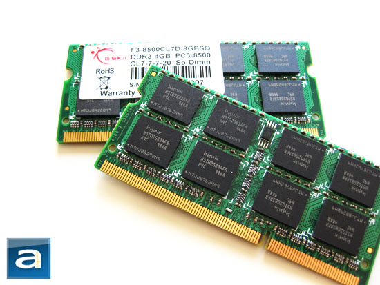
Each 4GB module of the G.SKILL F3-8500CL7D-8GBSQ kit features a six layer PCB with double sided memory chips. These 204-pin DDR3 SODIMMs are equipped with a total of sixteen Hynix H5TQ2G83AFR-H9C chips on both sides -- eight on each side of the board -- for maximum capacity. G.SKILL's modules are programmed to run at 1.5V, 533MHz actual clock (DDR3-1066/PC3-8500) with 7-7-7-20 latencies.
Specifications of the memory ICs are listed below, as obtained from Hynix's website:
The H5TQ2G43AFR-xxC, H5TQ2G83AFR-xxC are a 2,147,483,648-bit CMOS Double Data Rate III (DDR3) Synchronous DRAM, ideally suited for the main memory applications which requires large memory density and high bandwidth. Hynix 2Gb DDR3 SDRAMs offer fully synchronous operations referenced to both rising and falling edges of the clock. While all addresses and control inputs are latched on the rising edges of the CK (falling edges of the CK), Data, Data strobes and Write data masks inputs are sampled on both rising and falling edges of it. The data paths are internally pipelined and 8-bit prefetched to achieve very high bandwidth.
- VDD=VDDQ=1.5V +/- 0.075V
- Fully differential clock inputs (CK, /CK) operation
- Differential Data Strobe (DQS, /DQS)
- On chip DLL align DQ, DQS and /DQS transition with CK transition
- DM masks write data-in at the both rising and falling edges of the data strobe
- All addresses and control inputs except data, data strobes and data masks latched on the rising edges of the clock
- Programmable CAS latency 6, 7, 8, 9, 10, and (11) supported
- Programmable additive latency 0, CL-1, and CL-2 supported
- Programmable CAS Write latency (CWL) = 5, 6, 7, 8
- Programmable burst length 4/8 with both nibblesequential and interleave mode
- BL switch on the fly
- 8banks
- 8K refresh cycles /64ms
- JEDEC standard 82ball FBGA(x4/x8)
- Driver strength selected by EMRS
- Dynamic On Die Termination supported
- Asynchronous RESET pin supported
- ZQ calibration supported
- TDQS (Termination Data Strobe) supported (x8 only)
- Write Levelization supported
- Auto Self Refresh supported
- On Die Thermal Sensor supported (JEDEC optional)
- 8 bit pre-fetch

If you've never installed laptop memory before, it's quite a simple job. For those who are experienced, you'll understand that every laptop is designed differently, therefore the procedure for memory installation may also vary from a thirty second job to... well, a five minute job at most. My previous Dell Inspiron 6400 only required the removal of a dedicated RAM cover at the bottom of the chassis. However, my T400's memory modules are located underneath the palm rest, which requires the removal of four screws at the bottom of the laptop. This is probably as hard as it gets haha. The rest of the procedure involves unlatching the clips and removing the old SODIMMS, and installation is simply done by sliding the new RAM into their slot until it locks. By the way, the serial number is located on the label -- I just blanked it out in the photo above.

My "Pentium II" Lenovo ThinkPad T400.
For our benchmarks, our test system is configured as follows:
Laptop Model: Lenovo ThinkPad T400 (BIOS Revision 3.08)
CPU: Intel Core 2 Duo P8600 (Penryn 2.4GHz/3MB L2 cache)
Chipset: Intel Cantiga GM45 with ICH9M Southbridge (Montevina platform)
Display: 14.1" Samsung LED backlit LCD @ 1440x900
Graphics: ATI Radeon HD 3470 with Intel GMA X4500 - Switchable graphics
Hard Drive: Hitachi 5K320 250GB SATA
Wireless: Intel Ultimate WiFi Link 5300AGN
Operating System: Microsoft Windows 7 Professional x64
Compared hardware
- Qimonda (Stock Lenovo) PC3-8500 2x1GB @ 7-7-7-20
- G.SKILL F3-8500CL7D-8GBSQ PC3-8500 2x4GB @ 7-7-7-20
All tests were ran with the ATI Radeon HD 3470 dedicated graphics active, and Intel SpeedStep disabled with power options set to "High Performance" to obtain the most accurate benchmark scores.
1. Introduction, Packaging, Specifications
2. A Closer Look, Installation, Test System
3. Benchmark: EVEREST CPU
4. Benchmark: EVEREST FPU
5. Benchmark: EVEREST Memory
6. Benchmark: PCMark Vantage
7. Benchmark: 3DMark06 Professional
8. Benchmark: SuperPI, Cinebench R10; Conclusion