Page 3 - A Closer Look, Board Layout, Test System
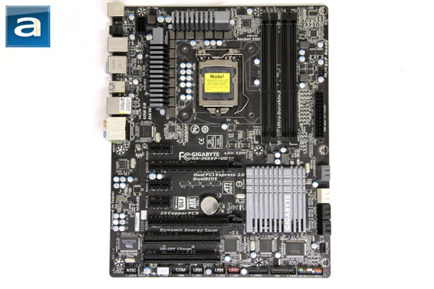
Taking a nice long look at the photo above, we can view the entire Gigabyte GA-Z68XP-UD3P in its profile shot. First off, the motherboard takes on a black PCB, much like the previously reviewed Gigabyte GA-P67-UD5. As stated in my colleague's review, we are definitely glad Gigabyte has decided to go for this classier design, rather than their previous ugly blue PCBs. All around the board, you will find black RAM slots, accompanied with black expansion card slots. As well, three separate gunmetal heatsinks are found covering the MOFSETs and the Intel Z68 platform controller hub. In terms of the overall aesthetics of the board, I would simply say the board looks a little plain. Of course, we aren't expecting the board to be particularly eye-catching and outgoing blue accents found on the UD5 model. In the end, physical aesthetics of a motherboard is not something I would consider crucial in the final rating, since, well, internal components do not get seen very often. I can, however, relate to those select individuals who use aesthetics as the final deciding factor when purchasing a new motherboard. Keep in mind that aesthetics are personal in opinion. Of course, the Z68XP-UD3P features all the bells and whistles found on many other Gigabyte performance motherboards, including 100% Japanese manufactured 50,000 hour solid state capacitors, ferrite core chokes, and lower RDS(on) MOSFETS for maximum durability and energy efficiency.
The Gigabyte Z68XP-UD3P motherboard takes on a mirrored L-shaped heatsink design that does not utilize any heatpipes. Unlike the higher end models that feature a C-shaped design, this motherboard uses smaller heatsinks, and covers only two of the four sides around the CPU socket in the middle. Of course, there is no central heatsink block found, which is fine, as the northbridge no longer exists. Also, none of the heatsinks are connected to each other, because there are no heatpipes on the Z68XP-UD3P. This simply means that each separate block is passively cooled on their own. We know most aftermarket CPU heatsinks will provide adequate cooling for the two blocks surrounding the CPU socket. The Z68 chipset heatsink will need to rely on airflow generated from your case fans, however.
Much like other motherboards of the same chipset, the ATX 4-pin/EPS 8-pin power connector is located at the top left corner of the motherboard. The layout is still fairly cramped, considering a 3-pin fan connector is sitting diagonally to the right of the power connector.

Above is a shot of the motherboard at the back. The design is relatively simple and clean; great for those thinking of adding aftermarket CPU cooling solutions. A standard Intel backplate is found here, but all LGA 1155 aftermarket coolers should be designed to work with this backplate in place. Along with the "Ultra Durable 3" scheme Gigabyte's performance motherboards are known to have, they also market the board to have two ounces of copper used on the power and ground layers of the PCB in order to improve both its cooling and power delivery efficiently to its components. This is done by lowering the PCB impedance. As shown in our image above, the use of surface mounts for the capacitors is evident. Around the board, pins still stick out for other components like RAM socket pins and expansion card slots; SMT (surface-mount technology) is not capable of withstanding higher mechanical stress required for this purpose.

Found around the LGA 1155 CPU socket is a host of components relating to the CPU voltage regulator circuit, including MOFSETs, capacitors, ferrite cores, and two heatsinks. Since the heatsinks are considerably smaller than many other motherboards, I have had no problems in installing large heatsinks with regards to its clearance. As stated above, the motherboard features ferrite core chokes and lower RDS(on) MOFSET transistors. The Gigabyte GA-Z68XP-UD3P also features a 12-phase dual CPU power VRM design. This design helps increase the power wattage delivery that in turn increases the overclocking performance. As well, since this motherboard is part of Intel's 6-series chipset, it utilizes Dual CPU Power delivery technology, which allows the voltage regulators ("Black blocks" in the photo above) to operate as two even sets of regulators. This dual power switch technology added with the Ultra Durable 3 marketing lingo is claimed to increase and improve motherboard reliability. Lastly, the Z68XP-UD3P also runs an Intel-approved VRD 12 compliant Intersil PWM controller. All these features work together to improve power usage and delivery, which optimizes efficiency, performance, and stability, while keeping temperatures lower.

The RAM slots on the Gigabyte Z68XP-UD3P are placed at a reasonable distance away from the CPU socket. Keep in mind the socket itself has been shifted to the right considerably from the older LGA 775 boards. Because of this, you may experience some clearance issues with the inner RAM slots if you utilize large aftermarket CPU heatsinks with high profile RAM heatspreaders. Since the new LGA 1155 socket, I had to remove the heatspreaders on one of my OCZ Platinum XTE PC3-16000 RAM sticks in order to utilize larger heatsinks. The ATX 24-pin power connector is placed along the right side of the Z68XP-UD3P with a 3-pin fan connector found just above it. Some things that are not found around this motherboard that are usually present on higher end models include an onboard power button, reset button, and clear CMOS button. This is to be expected with the UD3 line from Gigabyte.

Eight perpendicular Serial ATA connectors are found on the bottom right side of the Gigabyte GA-Z68XP-UD3P. The first six Serial ATA ports are native to the Intel Z68 chipset; while the last two are controlled by a Marvell 88SE9172 chip. The first six ports support RAID 0, 1, 5, and 1; while the last two only supports RAID 0 and 1. The first four Serial ATA ports that are colored black are SATA 3Gb/s connectors. The last four Serial ATA ports -- colored white and grey -- are SATA 6Gb/s connectors -- where the white ones are powered by Intel, and the grey ones are powered by Marvell. The Gigabyte Z68XP-UD3P motherboard does not feature any PATA or floppy connectors, which is fine, since the majority of users will not be using them in a modern system anyway.
The 3V CR2032 battery is placed between the SATA ports and 24-pin power connector, near the edge of the PCB. This is a good location for the battery, because it is not prone to physical obstruction by other components. To the left side of the array of SATA ports are the main BIOS and backup BIOS chips, respectively. If the main BIOS become corrupted, the system will automatically restore the image from the backup BIOS onto the primary BIOS. If the main BIOS become unusable for some reason (Such as physically damaged), the Z68XP-UD3P will automatically disable it, and the secondary BIOS will take its place.

The expansion slots, in order from the top, are: PCIe x1, PCIe x16, PCIe x1, PCIe x1, PCIe x16, PCI, and lastly, another PCI slot. The motherboard supports both CrossFireX and SLI. Although there are two PCIe x16 slots, the first PCIe x16 slot is the only real one. The second one will split up the bandwidth with the first slot if a second graphics card is used, creating two PCIe x8 slots. This is due to the limitations of the PCIe lanes provided by the Sandy Bridge core processors. However, do keep in mind that only the first PCIe x16 slot is a "true" PCIe x16 slot; the second one will do split it up with the first slot if a graphics card is installed to become two x8 slots. This is due to limited availability of PCIe lanes provided by Sandy Bridge core processors. Since the Z68XP-UD3P does not have a center heatsink, the top PCIe x1 slot will be able to support short and long cards. Also, the PCI slots found on the motherboard are connected to one of the PCI Express lanes by a PCIe to PCI Bridge.
The usual array of internal headers can be found at the bottom of the Z68XP-UD3P. From the left, we have a front panel audio header that supports Intel's high definition audio, S/PDIF Out Header, Firewire 1394 provided by a VIA VT6308 controller through the PCIe to PCI bridge, COMA Serial Port Header run by an ITE IT8728 controller, three sets of USB 2.0 headers for a total of six available ports controlled by the Z68 PCH itself, one of the two Etron EJ168 chips that power one available USB 3.0 internal header for a total of two available ports, TPM header, and lastly, the front panel case I/O header block. Also, above this block you will find the clear CMOS jumper.
Some miscellaneous chips found around the left side of this area include a Realtek RTL8111E chip for LAN, and a VIA VT6308 chip for Firewire. The main BIOS and backup BIOS chips are found just to the right of the "GIGABYTE GA-Z68XP-UD3P" text. Above the second PCIe x16 slot is a 3V CR2032 battery. Lastly, on the right side, under the Intel Z68 chipset and heatsink, is a PCIe to PCI Bridge chip, one of two Etron EJ168 chips, and an IT8728 controller.

The back I/O panel offers a large selection of connectors. The motherboard includes one dual purpose PS/2 connector provided by the ITE IT8728 chip, a large collection of eight red USB 2.0 ports, and a small host of two blue USB 3.0 ports. All USB 2.0 ports, including all internal headers and external connectors, are controlled by the Intel Z68 chipset. The two USB 3.0 ports are powered by one of the two Etron EJ168 ICs. The eSATA port is controlled by a Marvell 88SE9128 controller, and is capable of delivering power over the line. As well, the Z68XP-UD3P's USB ports are capable of providing up to three times the power from the standard 500mA spec to a total of 1500mA. Of course, this feature comes into handy a lot when dealing with hard drive enclosures that require more power to work. The USB 2.0 ports feature an on/off charge that allows the ports to deliver power, even when the system is turned off -- definitely a nice touch. One Firewire port is seen at the back powered by a VIA VT6308 controller through the PCIe to PCI bridge. A single Gigabit LAN port is controlled by the Realtek RTL8111E chip that is connected through a PCI Express lane. Lastly, the single optical connector and six 3.5mm analog jacks are controlled through Realtek's ALC889 audio codec.

Our test configuration as follows:
CPU: Intel Core i5-2500K @ 3.33GHz (Stock speed, Turbo Boost disabled)
CPU Cooling: Cooler Master Hyper 212 EVO
RAM: OCZ Platinum XTE PC3-16000 2x2GB
Graphics: Gigabyte Radeon HD 6850 1GB
Chassis: LanCool PC-K9
Storage: OCZ Vertex 2 60GB; 2 x Western Digital Caviar SE 320GB AAKS RAID1
Power: OCZ ZX Series 850W
Sound: Integrated (Motherboard)
Optical Drive: LiteOn iHAS224-06 24X DVD Writer
Operating System: Microsoft Windows 7 Professional x64
Compared Hardware:
- Gigabyte Z68XP-UD3P (Intel Z68, $190 at press time)
- ASUS P8P67 WS Revolution (Intel P67, $260 at press time)
- ASUS P8P67 PRO (Intel P67, $190 at press time)
- Gigabyte GA-P67A-UD5 (Intel P67, $260 at press time)
Page Index
1. Introduction, Features, and Specifications
2. Bundle, Chipset, BIOS
3. A Closer Look, Board Layout, Test System
4. Benchmark: AIDA64 CPU
5. Benchmark: AIDA64 FPU
6. Benchmark: AIDA64 Memory
7. Benchmark: PCMark Vantage
8. Benchmark: 3DMark 11
9. Benchmark: PassMark PerformanceTest 7.0
10. Benchmark: SuperPI 1M, Cinebench R11.5
11. Onboard Sound (RMAA 6.2.3) Analyzation
12. Overclocking and Conclusion