Page 2 - Intel Core i5-2405S Architecture; Test System
The first thing you will notice about the latest iteration of code-named Sandy Bridge processors from Intel, is the second generation Core i3/i5/i7 CPUs is housed in a new socket yet again. Ever since the release of Nehalem and Lynnfield core processors in 2008 and 2009, respectively, the company essentially segregated the market into two different distinct segments -- where owners of mainstream products are left with a dead end upgrade path; compared to the preceding Core 2 family, which uses a single socket in conjunction with universal chipset compatibility. To put it in simple terms in how this actually affects you, if you are considering upgrading to Sandy Bridge right now, you will need to cough up some cash for a new motherboard in addition to the CPU itself. The only bit of good news I have is LGA 1156 compatible aftermarket heatsinks will work without modifications on LGA 1155 motherboards. But do keep in mind Sandy Bridge processors in LGA 1155 are only mainstream to mainstream-performance units. Further down the road are LGA 2011 based Sandy Bridge processors to be released in Q4 this year. Main difference? Like Lynnfield core processors, chips such as the Intel Core i5-2405S we are reviewing today utilizes an updated version of DMI (Direct Media Interface) to connect to the Platform Controller Hub; aptly called DMI 2.0. DMI 2.0 doubles the transfer rate to 21Gb/s with a x4 link from DMI 1.0. LGA 1155 CPUs also retain the integrated dual channel DDR3-1333 memory controller found on Lynnfield core processors. LGA 2011 Sandy Bridge processors will feature QuickPath Interconnect (QPI) 4.8 GT/s to 6.4 GT/s, along with an upgraded native quad channel DDR3-1600 memory controller.
The current family of Intel Sandy Bridge Core i-series desktop processors include:
Core i7: i7-2700K, i7-2600K, i7-2600S, i7-2600
Core i5: i5-2500K, i5-2500S, i5-2500T, i5-2500, i5-2405S, i5-2400, i5-2400S, i5-2390T, i5-2320, i5-2310, i5-2300
Core i3: i3-2130, i3-2125, i3-2120, i3-2120T, i3-2105, i3-2102, i3-2100, i3-2100T
The 'K' suffix denotes unlocked multiplier, 'S' for a low power processor, and 'T' for an ultra low power processor.

One of the biggest highlights to the latest processors from Intel is an integrated GPU for the entire product line. While Intel has done so already for first generation Nehalem CPUs with the Clarkdale core, it was limited to products in the value segment only; and in practice it was just a 45nm GPU and 32nm CPU core consolidated into a single chip package. Sandy Bridge takes on a much more elegant approach from an engineering perspective. Intel merged these two parts together on the die, with both the CPU and GPU created using their 32nm fabrication process. Since all Sandy Bridge CPUs now come with a 'free' GPU, it is up to the chipset and motherboard manufacturer to enable this feature. We will cover that in just a short moment. Some companies like to say The Future is Fusion. In my opinion, AMD's got that right. For Intel.
Along with the added features, this monolithic piece of silicon now packs 995 million transistors under the hood -- up from 774 million from last generation Lynnfield core processors. Combined with Intel's High-K metal gate technology, everything is packed into a die size of only 216mm². This brings us to the diagram above, which gives a nice microscopic view into the physical layout of Sandy Bridge CPUs. 32KB of 8-way cache for both data and instruction makes up the 64KB L1 cache; followed by 256KB of 8-way L2 cache per core for a total of 1024KB combined. The 12-way L3 "Smart Cache" is pooled in the middle so it can be used by both the processor cores and the integrated graphics core as aforementioned simultaneously. Sandy Bridge Core i5 processors such as the 2405S we are reviewing today have 6MB cache; while Core i3s and Core i7s carry 3MB and 8MB, respectively.
Before we move on any further into the details of what's going on inside the CPU, let's get the bad news out of the way first. Intel uses a single clock generator to control the speed of all electrical buses in all Sandy Bridge processors. Overclocking in the past decade or so involved raising your CPU's FSB/base clock/whatever to squeeze extra clock cycles out of it. You can't do that anymore with Sandy Bridge, because by raising the base clock, you are overclocking every other component inside the chip -- and many parts are not very overclockable at all. Enthusiast K-series chip like the Intel Core i5-2500K we have reviewed a few months ago has an unlocked multiplier up to 57x. This creates a theoretical ceiling of 5700MHz (57*100), but you'll hit your physical limit way before that happens. If you don't have a K-series CPU like this one, then you have no choice but stick to stock frequencies. Gone are the days where you can buy a cheap Intel processor and overclock the crap out of it.
Second generation Intel Core i5s like the 2405S we are reviewing today has four physical cores. The 'S' indicates a reduced TDP from 95W to 65W. Meanwhile, second generation Core i3s will have two physical cores with Hyper-Threading. Like previous generation Nehalem processors, the main difference between Core i5 and i7s, other than quantity of cache, is that the latter supports Hyper-Threading for up to eight simultaneous threads (Four physical cores and four logical cores). Media related multithreaded applications optimized for Hyper-Threading will benefit the most from this technology, but in many other cases, the lack of such will not affect performance to a significant degree.
The AVX (Advanced Vector Extensions) instruction set on Sandy Bridge is the last thing I want to talk about before moving onto its on-die graphics processor. You will need Windows 7 Service Pack 1 along with compatible applications to take advantage of its incredible performance increase in this area due to a change of format from XMM to YMM. AVX is basically an advanced version of the Streaming SIMD Extension (SSE) instruction set. Not only does it take the chip's SIMD vector register data path width from 128 bit to 256 bit, and increase its operand instruction limit from two to three -- Intel claims the AVX extension will execute non-native instructions faster as well.
Since Intel Sandy Bridge CPUs have an integrated graphics processor inside, let's talk about it in a little more detail. This IGP is called the Intel Graphics Media Accelerator HD; which unsurprisingly is based off existing Intel graphics solutions -- but with numerous improvements. The Intel Graphics Media Accelerator HD is a DirectX 10.1 (Sorry guys, no DX11) compatible GPU with 6 execution units per core. Intel's Graphics Media Accelerator HD 3000 like the one found in our Core i5-2405S has two cores for 12 execution units in total; while the Core i5-2400S has Intel's Graphics Media Accelerator HD 2000 IGP, which has one core for 6 execution units in total. Each execution unit is able to handle twice the amount of work per clock cycle compared to the IGP found in Clarkdale processors. The GPU operates at 850 MHz by default.
Do keep in mind that while it is faster than previous generation integrated graphics, don't expect to dump your expensive AMD or NVIDIA cards and expect decent framerates in return anytime soon. This is an entry-level gaming solution at best; but Intel would like you to consider it as a media processor rather than a gaming solution. Where it really shines is its video processing capabilities. With its dedicated logic for video encoding and decoding tasks, playback wise, thanks to its HDMI 1.4a implementation, it is very good for Blu-ray and even stereoscopic 3D. Transcoding wise, it is fully performed in hardware with a fixed function multi-format codec architecture to speed up video processing performance.
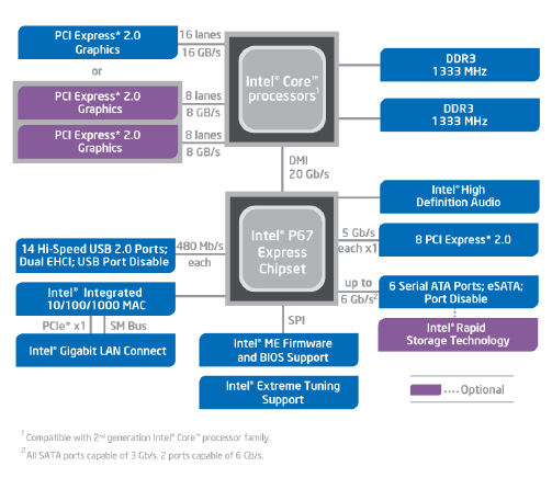

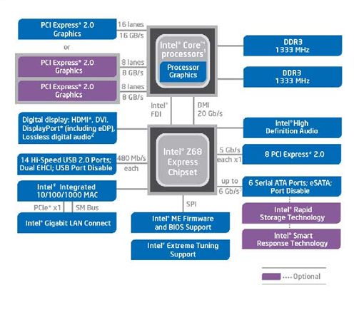
Three chipsets designed for Sandy Bridge processors are available to consumers at press time. Codenamed Cougar Point, the H67 is aimed at mainstream consumers who are not interested in overclocking, but want to take advantage of the integrated graphics. Enthusiasts who want to overclock or use multi-GPU configurations will need to buy motherboards based off the P67 chipset. The Intel Z68 consolidates the best of both worlds, and adds SSD caching to the features list. Common to H67, P67, and Z68 is UEFI support -- pretty much the first time this has hit mainstream with desktop PCs. The biggest advantage to UEFI motherboards are 3TB+ HDD support, more flexible network booting, and much nicer GUIs for the setup screen. As with first generation Core family CPUs, what was previously known as the Southbridge now takes care of the standard connection interfaces such as providing up to 14 USB ports and 6 SATA ports (Of which two of them are SATA 6Gb/s), as well as providing eight additional PCI Express lanes for PCIe based devices such as Ethernet. There is no native USB 3.0 support, so it will still go through a third party controller. Because many Northbridge functions are now on the CPU itself as aforementioned, P67 and Z68 chipsets didn't do nearly as much as it did in the past -- thus, Intel has resolved to call it the Platform Controller Hub, or PCH, just like the P55.
On the topic of Intel's January Cougar Point recall, one of the transistors inside the Serial ATA 3Gb/s ports in B2 stepping of the chipsets are receiving more voltage than it should, and will degrade over time. The SATA 6Gb/s ports are not affected. Users with high I/O workloads on their SATA 3Gb/s ports will speed up this problem. The degradation will come in the form of increased data transfer error rates; eventually resulting in complete device connection loss. Intel claims that this problem will only affect 5% of users over 3 years, but the has issued a recall on January 31st, 2011 and all major motherboard and computers manufacturers have then stopped shipping motherboards with the faulty chipset. A little more than a month later, B3 revision chipset began shipping, and manufacturers want to make it clear to the consumer which motherboards are fixed, and which ones are not. You can see how it was worked out in our past P67 motherboard reviews, such as the ASUS P8P67 WS Revolution, ASUS P8P67 PRO, and Gigabyte GA-P67A-UD5 reviews. But at this time of the year, there is absolutely nothing to worry about in this regard.
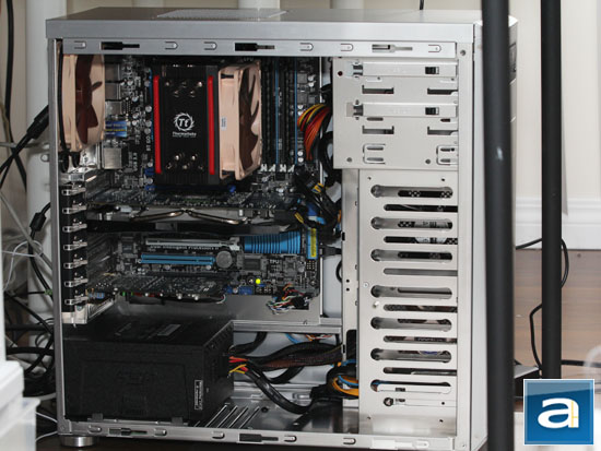
Our test configuration as follows:
Compared Hardware:
- Intel Core i5-2405S @ 2.50 GHz (Stock speed, Turbo Boost disabled) on ASUS P8P67 PRO
- Intel Core i3-2120 @ 3.33 GHz (Stock speed) on ASUS P8P67 PRO
- Intel Core i5-2500K @ 3.33 GHz (Stock speed, Turbo Boost disabled) on ASUS P8P67 PRO
- Intel Core i5-750 @ 2.66 GHz (Stock speed, Turbo Boost disabled) on ASUS P7P55D-E Premium
Common Specifications:
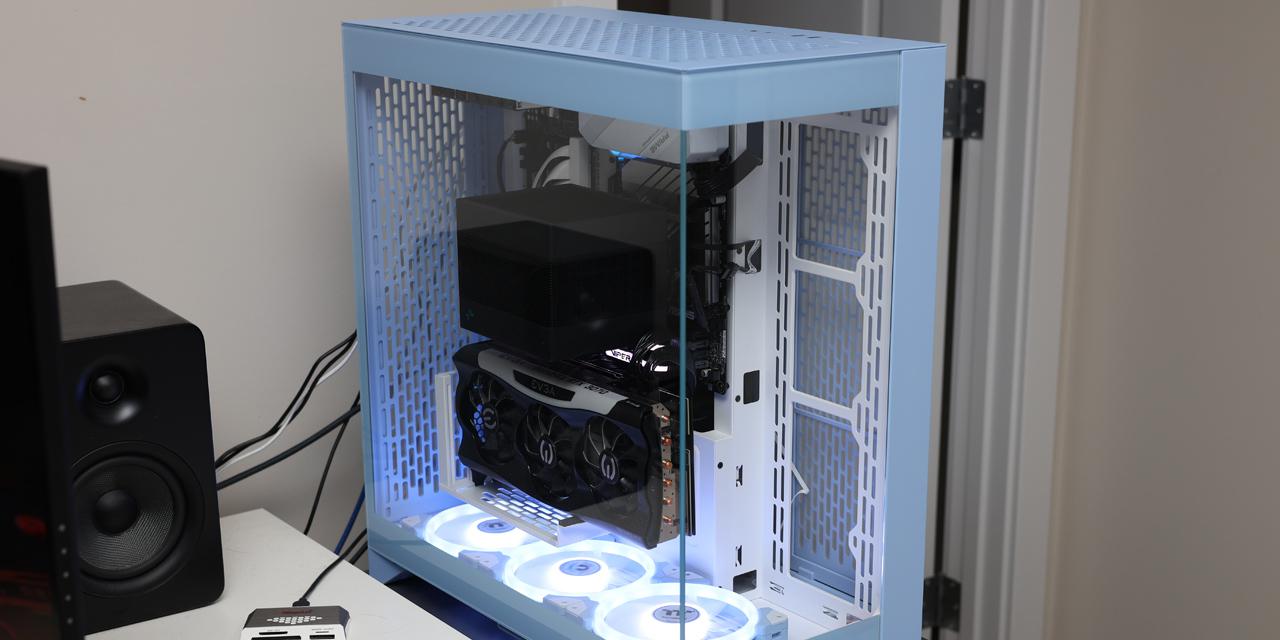
Cooling: Thermaltake Frio with Noctua NF-P12
RAM: G.SKILL Ripjaws F3-12800CL7D-8GBRH 2x4GB @ DDR3-1333 7-8-7-24 (Reduced frequency @ stock latencies)
Graphics: Gigabyte Radeon HD 6850 1GB
Chassis: Lian Li PC-Z60 (Noctua NF-S12B ULN)
Storage OCZ Vertex 2 160GB 25nm; Western Digital Scorpio Blue 500GB
Power: FSP AURUM CM Gold 650W
Operating System: Microsoft Windows 7 Professional x64 SP1
Page Index
1. Introduction and Specifications
2. Intel Core i5-2405S Architecture; Test System
3. Benchmark: AIDA64 CPU
4. Benchmark: AIDA64 FPU
5. Benchmark: AIDA64 Memory
6. Benchmark: BAPCo SYSmark 2007
7. Benchmark: PCMark Vantage
8. Benchmark: 3DMark 11
9. Benchmark: PassMark PerformanceTest 7.0
10. Benchmark: SuperPI 1M, Cinebench R11.5
11. Power Consumption and Conclusion