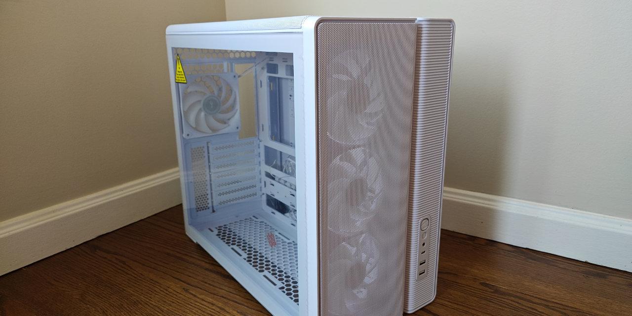
Page 3 - A Closer Look, Board Layout, Test System

In classic ASUS style is the P8P67 WS Revolution built on a beautiful black colored printed circuit board. Consisting primarily of blue, black, silver, and grey components, the end result is excellent as always. I have always been a big fan of the way ASUS motherboards look (Especially in my windowed case), and this one is certainly no exception. While aesthetics is not really an issue when it comes to internal components of a computer compared to the way the board is built and how well it performs, surprisingly it can be a deciding factor for some users. Of course, the comments on the look are just a personal opinion. As it has gained immense popularity for the last couple years, the ASUS P8P67 WS Revolution, like many performance motherboards in the industry, features 100% Japanese manufactured solid state capacitors, lower RDS(on) MOSFETS for maximum durability and energy efficiency. Along with the company's DIGI+ VRM, ASUS claims an efficiency of up to 92%. Of course, we don't have the means of testing this independently, nor do we know exactly how this figure is obtained, but we will take their word for it.
As you can see the design of the heatpipes above, it is a little more than just an L-shaped heatpipe. The silver/grey colored copper heatpipes arrives in an industry-standard C-shaped design which can be seen at the top, where heat dissipation is implemented over components in three of four sides of the CPU socket in the middle. Wait a second... didn't you say that P67 does not have a Northbridge and Southbridge? That is correct -- the bottom end section of the heatpipe system begins with a small silver block to bring additional cooling over P67 platform controller hub. The central block resides over the NVIDIA NF200 bridge chip that provides additional PCI Express lanes to the graphics slots. From there, it leads on to the main build via a single heatpipe. The heatpipe continues on from the central P67 PCH cooler directly to the first array of cooling fins for heat dissipation out the back -- this is taken advantage of when airflow is brought over this area by the rear exhaust fan in a standard chassis, as well as the CPU cooler. During our tests, the heatpipe system worked well and adequately cooled our P67 chipset even under overclocking scenarios in my low airflow silent setup.
As with its predecessors, the ATX 4-pin/EPS 8-pin power connector is located at the top left corner of the motherboard, behind the second pair of USB ports. It is fairly cramped in that area, especially considering adjacent to the power connector are several other components. It is not as hard to disconnect once the ATX 4-pin/EPS 8-pin connector is clipped in, as compared to the past -- however, shuffling the components around to make the connector face up would have been easier on the end user.

A shot of the back of the motherboard. A very clean design; for those who are going to install aftermarket heatsinks with proprietary backplates, rest be assured there is absolutely nothing to worry about. What you will find is the standard Intel backplate, but all heatsinks designed for LGA1155 should be designed to work with the backplate in its place. Two ounces of copper were used on the inner layers of the P8P67 WS Revolution to improve its cooling efficiency by spreading the heat out more evenly, as well as delivering more power more efficiently to its components by lowering the PCB impedance. (Sounds familiar? Gigabyte advertises this, too.) Regarding the use of capacitors, the use of surface mounts is evident, as shown in the image above. Pins still stick out for other components, for example, the RAM socket pins and PCIe slots -- since SMT is not capable of withstanding higher mechanical stress required for this purpose.

Within close proximity of the LGA1155 processor socket is the usual array of items -- components relating to the CPU voltage regulator circuit, as well as heatsinks from the heatpipe loop. The components in general are relatively low profile, so I have experienced no problems in installing large heatsinks such as the Noctua NH-D14. As shown in our photo above, you will see one of the biggest things ASUS advertises in their P8P67 line of motherboards. Rather than using traditional analog voltage regulation system, the company takes it a step further and uses an Intel VRD12 compliant digital 16+2 phase power design. Marketed as DIGI+ VRM, it allows a higher level of precision when it comes to power delivery, faster transient response, reduced power loss, and reduced electromagnetic interference with spread spectrum enabled. This works in conjunction with the Energy Processing Unit (EPU) ASIC and TurboV Processing Unit (TPU) hardware controller to mesh component monitoring, automatic power management, and accurate user control together. I think this is quite brilliant, because stuff like the EPU and TPU are nothing new to us -- but now they all work together on a hardware level. In the end, if all these terms mean nothing to you, it is okay -- all you need to know is we can now take a crack at better overclocks along with improved system stability.

The RAM slots are placed a reasonable distance away from the CPU socket, but since the CPU socket is shifted to the middle of the board rather than left biased like old LGA 775 boards, you may experience clearance issues with the inside slots if you have memory with tall heatspreaders in conjunction with a large CPU heatsink/fan. The ATX 24-pin power connector is placed along the side of the motherboard as far as standard design is concerned, but a good number of user accessible functions are placed adjacent to it as well. From the top, we have a TPU switch, MemOK! button, 3-pin PWR_FAN header, EZ Plug, USB header, and another 4-pin CHA_FAN header. The EZ Plug is a 4-pin Molex connector used to deliver additional power to your motherboard (Connection is fully optional though). Placement of USB 2.0 headers in this area is also quite unconventional, but can definitely come in handy for neat cabling of chassis front panel USB ports.
The MemOK! button allows the user to auto start the system in working with the memory in the pre-post state by first attempting relaxing the timings, followed by adjusting frequency, and finally increasing the voltage to allow the system to POST. This is very beneficial, since there may be boot issues with higher voltage memory kits or otherwise problematic memory -- and users won't be stuck looking for standard voltage memory in order to modify settings in their BIOS just to start their system. Overclockers may also find this feature beneficial by using MemOK! to reset their memory settings only, rather than resorting to clearing the CMOS.

Eight color coded Serial ATA connectors are angled perpendicular to the motherboard for optimal cabling convenience. The first six SATA ports are native to the P67 chipset; and supports RAID 0, 1, 5 and 10. The grey ports are SATA 6Gb/s ports, while the blue ports are SATA 3Gb/s ports. The navy blue ports are provided by the Marvell 9128 PCIe SATA 6Gb/s controller, which supports RAID 0 or RAID 1. You can see the chip right next to the ports. ASUS' P8P67 WS Revolution motherboard does not feature any legacy PATA or floppy connectors, which in my opinion it is about time we got rid of them, haha.
The BIOS chip is situated on the right side of the Intel SATA 6Gb/s ports in reference to our above photo. Meanwhile, the case I/O connector pin layout is standard amongst all ASUS motherboards, and out of the box it comes with ASUS' Q-Connector block to combine all the mess into a neat single block for maximum convenience. Good placement of connectors in this segment of the motherboard is usually very challenging, and ASUS has done an excellent job of organizing it in an efficient and user friendly manner.

The expansion slots, in order from the top, are: PCIe x16, PCIe x1, PCIe x16, PCIe x1, PCIe x16, PCIe x1, and another PCIe x16 slot. Notice how there are no legacy PCI slots. The ASUS P8P67 WS Revolution takes the best of both worlds and supports both CrossFireX and SLI. Additionally, thanks to the NVIDIA NF200 chip, there are more PCI Express lanes available to these slots than what the Sandy Bridge core processors are able to provide on chip. You can also have your own CUDA setup with up to four NVIDIA Tesla GPUs. Both blue slots can operate at full bandwidth concurrently, but you will need to do a half-split with the black slots if you want those in service too. In other words, your P8P67 WS Revolution can do x16/none/x16/none, or x8/x8/x8/x8. This is more than enough for 99% of the users out there. Another great thing to note is each PCI Express x16 slot is separated by a PCI Express x1 slot in between, so you can actually install four dual slot graphics cards. This is very important, because any graphics card of decent performance nowadays will occupy two slots. My only concern is the top PCIe x16 slot, while not obstructed by any chipset heatsinks in length, will put your video card really close to uber large heatsinks sitting over your processor. I still have enough clearance with my NH-D14, but the clearance room is literally less than a couple millimeters at the closest point.
An array of internal headers and switches can be found at the bottom of the P8P67 WS Revolution. From the left, we have Firewire provided by the VIA VT6315N PCIe based host controller, EPU switch, USB 2.0, serial port, TPM (We'll cover this in just a short moment), and a 4-pin CHA_FAN. All fan headers on this motherboard is capable of controlling both 3-pin voltage and 4-pin PWM fans. A chassis fan mode selection jumper can be found next to the ones used to clear CMOS, but I don't see why they can't just make it a BIOS option instead -- Gigabyte has that in the P67A-UD5.
At this point, you may be wondering why I tiptoed around the two external USB looking ports on the P8P67 WS Revolution. For one thing, I am not tiptoeing around this topic -- I'll cover it now. Secondly, those external USB looking ports are, in fact, external USB 2.0 ports. What are they doing here? They're used for components that are permanently attached to the system, and you don't want to risk having them knocked out. This may include USB WiFi adapters, flash drive for ReadyBoost, and the such.
Miscellaneous chips spotted in our photo above include a Nuvoton NCT6776F monitoring chip, TurboV EVO controller, and a CR2032 3V battery between the two PCIe x16 slots. Along the western edge, from the top, is the NEC USB 3.0 controller, Intel 82579V Gigabit LAN controller, VIA VT6315N Firewire controller, and Realtek ALC889 audio codec.

One special feature on ASUS' P8P67 WS Revolution is the G.P. Diagnosis Card. It is a detachable board that plugs into the TPM connector on your motherboard, and has three things on there: A two digit LCD display, power button, and reset button. In the past, we have seen the latter two features integrated right onto the motherboard, while Gigabyte features all three without a detachable module in their flagship products. As its name suggests, it is particular useful for diagnosing problems -- the LCD display will show a code corresponding to a table in your manual to indicate what is going on during POST. For example, code 32 means early CPU utilization. If it freezes at this point, you will know what you should focus on.

ASUS offers a generous amount of available external connectors at the back panel. Notably missing are the eSATA ports, but what you get instead is a serious load of USB ports. From the left, we have a PS/2 port for either a keyboard or mouse (This is good, because I'd rather take an extra two USB ports than dedicated connectors for both PS/2 keyboard and mouse), two USB 2.0 connectors in black, one coaxial and one optical audio output, four more USB 2.0 connectors in black, two Intel Gigabit LAN ports with one VIA VT6315N powered Firewire connector placed in between, and two NEC powered USB 3.0 connectors in blue. Yep, ten USB ports in total. Impressive. The rest are audio connectors based off the Realtek ALC889 audio codec; both S/PDIF coaxial and optical outputs can be seen as aforementioned in addition to the six standard 3.5mm analog jacks. An EMI shielded I/O backplate, which ASUS calls the "Q-Shield", accompanies the motherboard.
I am very happy to see Intel Gigabit LAN ports on the P8P67 WS Revolution, rather than Realtek or Marvell based adapters we have seen on pretty much every motherboard for the last little while. ASUS' marketing material says Intel's solution provides lower CPU utilization, but from my perspective, I could care less -- a few extra clock cycles on my Sandy Bridge processor won't make a difference. What really gets me excited is the fact that Intel's Gigabit LAN controllers deliver significantly better performance than the competition, as I have discussed in my QNAP TS-559 Pro+ review last year. For network attached storage obsessed people like me, this makes a big different when you are moving hundreds of gigabytes through your network at a time.

During operation, four blue LEDs surrounding the ASUS logo fades in and out.
If you really don't want to go through all the benchmark results, Page 10 has something that is thoroughly convincing. I promise.
Our test configuration as follows:
CPU: Intel Core i5-2500K @ 3.33GHz (Stock speed, Turbo Boost disabled)
CPU Cooling: Noctua NH-D14
RAM: G.SKILL Ripjaws F3-12800CL7D-8GBRH 2x4GB @ DDR3-1333 7-8-7-24 (Reduced frequency @ stock latencies)
Graphics: Gigabyte Radeon HD 6850 1GB
Chassis: Cooler Master 690 II Advanced NVIDIA Edition (Noctua NF-S12B FLX, NZXT Sleeved LED Kit)
Storage: OCZ Vertex 2 60GB; Western Digital Caviar Blue AAKS 500GB
Power: NZXT HALE90 750W
Sound: Auzentech X-Fi HomeTheater HD
Optical Drive: LiteOn iHAS224-06 24X DVD Writer
Operating System: Microsoft Windows 7 Professional x64
Compared Hardware:
- ASUS P8P67 WS Revolution (Intel P67, $260 at press time)
- ASUS P8P67 PRO (Intel P67, $190 at press time)
- Gigabyte GA-P67A-UD5 (Intel P67, $260 at press time)
Page Index
1. Introduction, Features, and Specifications
2. Bundle, Chipset, BIOS
3. A Closer Look, Board Layout, Test System
4. Benchmark: AIDA64 CPU
5. Benchmark: AIDA64 FPU
6. Benchmark: AIDA64 Memory
7. Benchmark: PCMark Vantage
8. Benchmark: 3DMark 11
9. Benchmark: PassMark PerformanceTest 7.0
10. Benchmark: SuperPI 1M, Cinebench R11.5
11. Onboard Sound (RMAA 6.2.3) Analyzation
12. Overclocking and Conclusion